Semiconductors are essential components in many modern technologies, including computers, digital cameras, LEDs, automobiles, and solar panels. Despite their prevalence, current methods to produce semiconductors are energy intensive and costly.
Researchers working with Bryce Sadtler, associate professor of chemistry in Arts & Sciences, and Rohan Mishra, associate professor of mechanical engineering & materials science in the McKelvey School of Engineering, both at Washington University in St. Louis, recently developed an alternative method for producing semiconductors.
The team’s novel approach uses electrodeposition to create a thin layer of material without the need for an expensive and difficult to produce subsurface. The method could reduce the cost of growing semiconductors and improve the accessibility and scalability of the process.
The results were published Sept. 29 in the Journal of the American Chemical Society.
“A major challenge in making high-quality semiconductors using electrodeposition has been the need for a single-crystalline substrate, or subsurface for the semiconductors to grow on,” Sadtler said.
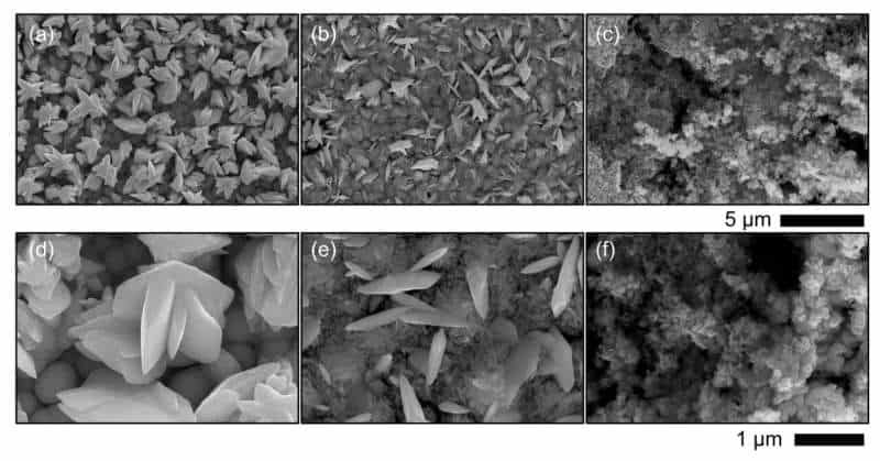
“Our work developed a strategy to use electrodeposition to synthesize the semiconductor compound without the need for a single-crystal substrate,” explained first author Jiang Luo, a graduate student working with Sadtler and Mishra. “We found that under the right growth conditions, a seed layer forms during the early stages of electrodeposition that can produce a polycrystalline film of sufficient quality for semiconductor devices.”
The team’s novel mechanism to grow high-quality semiconductor films relies on that initial seed layer, which Luo and Sadtler said was unexpected but ultimately essential to control the growth and final structure of the semiconductor film.
“Once we figured out the importance of the seed layer, we used this mechanism to successfully electrodeposit films of the semiconductor bismuth selenide on both single-crystal substrates and substrates that are not single crystals,” said Luo. “We believe this novel mechanism of seeded electrodeposition can be extended to other semiconductors that are currently difficult to synthesize.”
Looking ahead, the team anticipates that their method for producing semiconductors may be attractive for new applications in green energy, quantum computing, and biomedical imaging. The semiconducting material used in this study, bismuth selenide, has several properties that make it particularly appealing for these emerging applications.
“The ability to produce semiconductor films like bismuth selenide by electrodeposition at room temperature without the need for a single-crystal growth substrate can facilitate the incorporation of these materials into devices for energy and information conversion,” Sadtler said.
“One specific application for the films synthesized in this work is to make cameras that are sensitive to the polarization of light. Typical cameras detect only the brightness and color of light. The ability to also detect the polarization (or orientation) of light provides additional information that could be used for the early detection of certain types of cancer.”